Convert Schematic To Pcb Altium
Design pcb schematic and layout in altium by sociallyvegan Embedded system engineering: altium designer tutorial 3 How to convert pcb to schematic diagram?
Embedded System Engineering: Altium Designer Tutorial 3 - Circuit Schematic
Pcb schematic diagram layout easyeda convert into Easyeda software convert presented Altium fiverr
Altium schematics fiverr screen
Tutorial schematic altium pcb designer embedded engineering system continue layout next make willPcb altium layout supply power embedded engineering system 3v layer example double just How to create a pcb layout from a schematic in altium designer1 hour tour about altium designer(schematic-pcb designing).
Embedded system engineering: altium designer tutorial 4Schematics according restore raypcb convert orcad protel Pcb guideline altiumDesign schematic and pcb in altium by wangdegang.
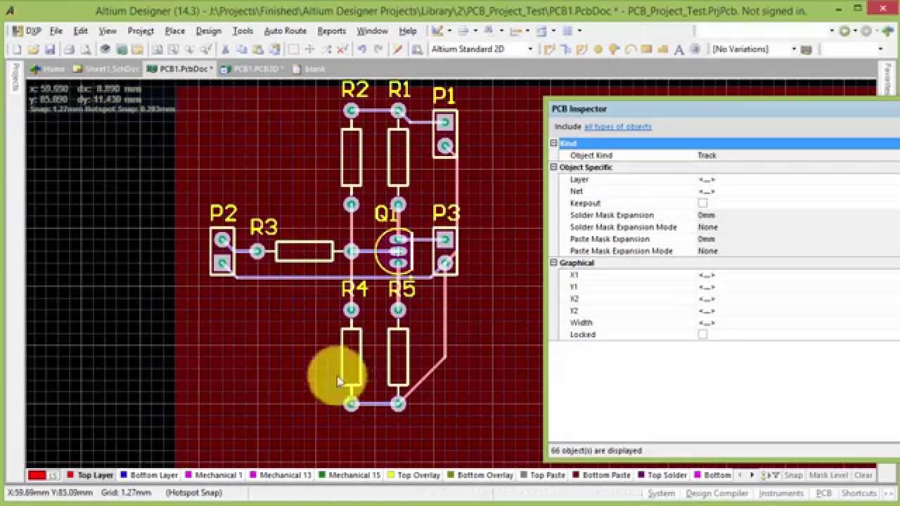
Altium pcb learning week schematic monitors both complete left board
Design schematics and pcb in altium by faiz07How to convert pcb to schematic diagram? Altium pcb schematic screen fiverrHow to convert schematic diagram into pcb layout in easyeda online pcb.
Learning pcb design in one weekGetting started with easyeda part 3: pcb layout .


Design schematics and pcb in altium by Faiz07 | Fiverr

Design schematic and pcb in altium by Wangdegang | Fiverr

Getting Started with EasyEDA Part 3: PCB Layout - Shawn Hymel

Learning PCB design in one week - We have the Technology

How to Convert PCB to Schematic Diagram? - RAYPCB
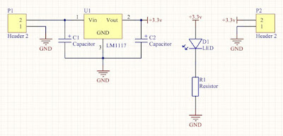
Embedded System Engineering: Altium Designer Tutorial 3 - Circuit Schematic

Embedded System Engineering: Altium Designer Tutorial 4 - PCB Layout

How to Convert schematic diagram into PCB layout in Easyeda Online PCB

How to Convert PCB to Schematic Diagram? - RAYPCB

Design pcb schematic and layout in altium by Sociallyvegan | Fiverr